

Next week, Intel will present papers on the Gate-All-Around (GAA) RibbonFET and PowerVia. Due to its discussion of Backside Power Delivery Network (BS-PDN) technology, the latter is likely to be the blue chipmaker’s one-two punch.
According to Ryan Smith of Anandtech, Intel has been discreetly investigating the PowerVia Backside Power Delivery Network for years. Its development is comparable to EUV, although Intel may let other chip fabs to utilize it soon.
Intel’s Next-Generation PowerVia Processors To Hit Stores In 2024
PowerVia BS-PDN operates like this: Modern processors with frontside power supply include 10–20 metal layers. The Intel 4 CPU will have 16 logic layers and two “giant metal” layers for power routing and external interfaces.
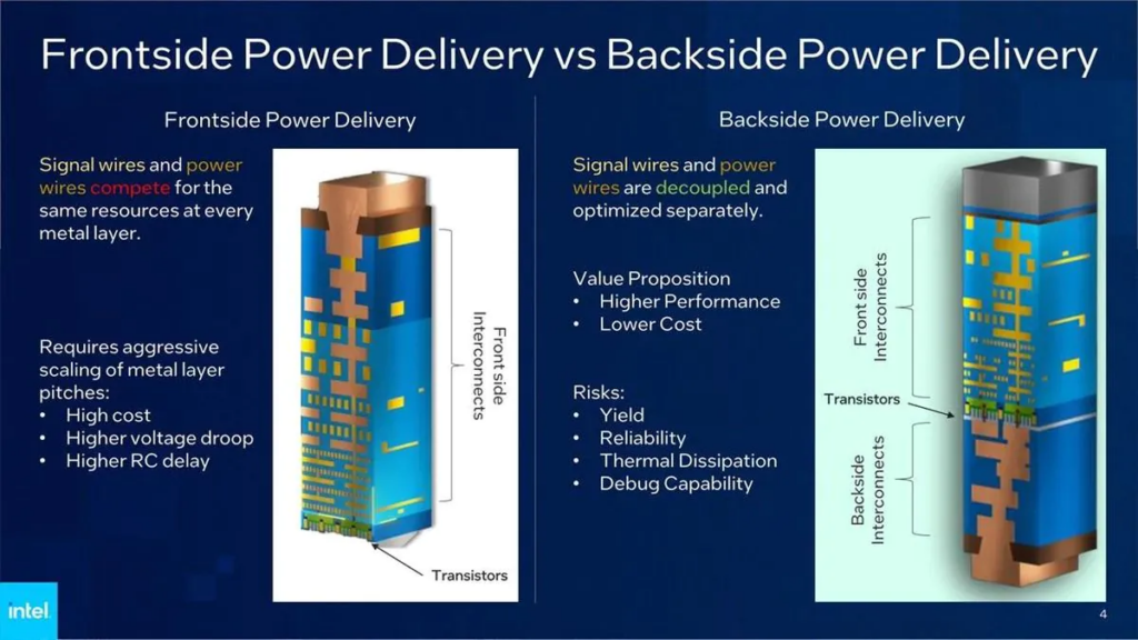
Since transistors and signals are on the same side of the device, frontside power delivery requires signals to go through layers to reach them. Intel separates such signals by transferring all chip power connections to the other side of the wafer with backside power delivery.
Intel employs Nano TSV for PowerVia BS-PDN. The “TSV”—through-silicon via—directs electricity to a processor’s M0 layer instead of passing through it. It involves stacking silicon layers over the primary chip.
If this sounds familiar, it’s because AMD’s 3D V-Cache technology is comparable. Nano TSVs are 500 times smaller than standard TSVs. A 30% reduction in voltage droop allowed the CPU to run at lower voltages while improving performance.
Intel also stated that PowerVia with its BS-PDN is operating and that “Blue Sky Creek” test chips, created using a modified version of its Intel 4 technology, had begun mass production. Intel would have bragging rights if the technology succeeds as none of its competitors are likely to have backside power delivery available by 2026.